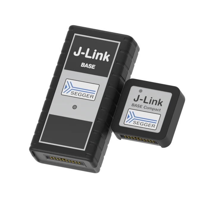
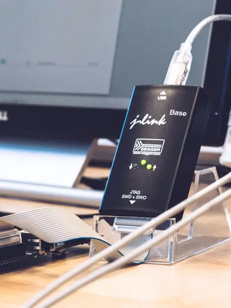
J-Link BASE
The entry-level debug probe
- Cost-effective entry into professional debugging with SEGGER’s proven J-Link platform
- Reliable performance for standard development across a wide range of devices
- Basic feature set, with advanced capabilities available in higher-tier models
Key features

High download speeds
J-Link BASE offers download speeds of up to 1 MB/s, ensuring that project development moves forward smoothly and reliably, with minimized download times.
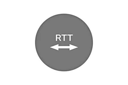
Real Time Transfer
J-Link BASE offers Real Time Transfer (RTT), which provides a simplified path for information to travel when an application is running. Users can also easily monitor changes in operation.
Broad CPU and IDE support
J-Link BASE works with an extensive range of microcontrollers and IDEs. It enables users to connect their selected microcontroller with their favorite IDE.
Note
Compared to higher-end J-Link models, the J-Link BASE offers a reduced feature set. Advanced capabilities such as download speeds of up to 4 MB/s, unlimited breakpoints in flash memory, and support for tools like Ozone and J-Flash available in higher-tier models.
For full access to SEGGER’s debugging ecosystem and maximum performance, we recommend models such as J-Link Pro or J-Link Ultra.
Supported devices
The list of supported manufacturers, families, devices, and systems on a chip includes tens of thousands of devices in hundreds of device families.
Device not listed? Please don’t hesitate to contact us.
Use cases
Entry-level debug hero
J-Link BASE is a modern debug probe that is both smart and a swift communicator, which means communications are carried out not only reliably, but also faster than with a simpler probe. SEGGER's RTT debug communication interface is also available, and all popular IDEs offer support for J-Link.
Basic debug support
Should a toolchain not support the comprehensive feature set, including unlimited breakpoints in flash memory and monitor-mode debugging, found in the more-advanced J-Link products, J-Link BASE is a sensible, cost-efficient alternative for use with OpenOCD or similar tools.
Upgrade path
J-Link BASE offers basic functionality. To use the full range of features found in a J-Link PLUS, for example, the J-Link BASE to PLUS upgrade is required.
This upgraded license includes a software bundle with a J-Flash/J-Flash SPI software license to program EEPROM and flash chips in microcontroller systems, and a J-Link Unlimited Flash Breakpoints license. Also included is the Ozone debugger and performance analyzer, monitor-mode debugging technology, and a license pack for the RDI interface.
J-Link's BASE to PLUS upgrade is available at shop.segger.com.
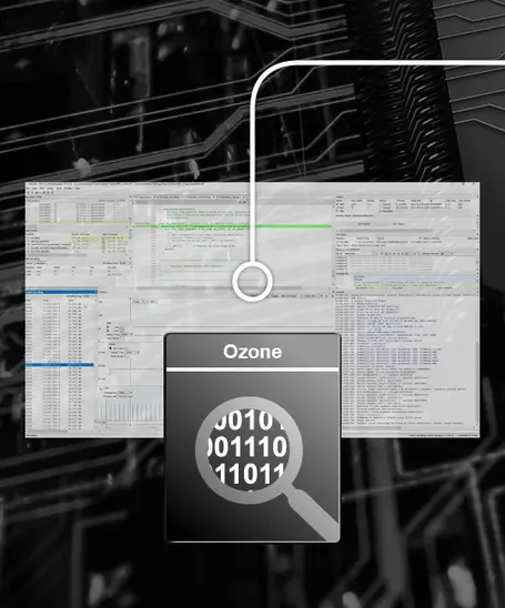
Ozone
Ozone is a professional, full-featured standalone graphical debugger for embedded applications that is capable of debugging the output of any toolchain or IDE. It includes all common debug controls and information windows. Furthermore, it enables high-speed application-to-target programming and debugging of information windows for any purporse, including disassembly, memory issues, and more. Ozone is available with J-Link PLUS, PRO, PRO PoE, and ULTRA+.
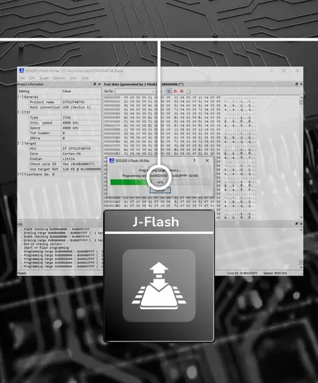
J-Flash
J-Flash enables programming of microcontroller internal and external flash memories. Exceedingly versatile, it runs on Microsoft Windows, Linux, and macOS, and it supports Cortex Arm, RX, and Power PC devices and cores. For all members of the J-Link and J-Trace families positioned above J-Link BASE, J-Flash is included in the J-Link Software and Documentation Package.
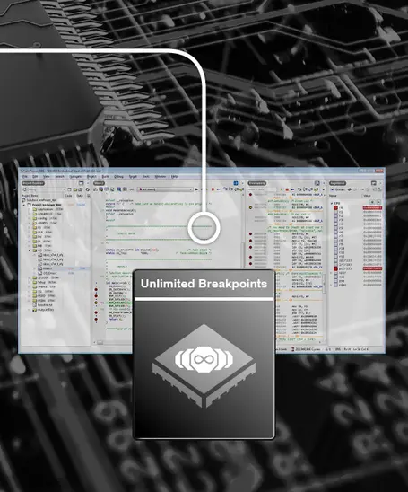
Unlimited breakpoints
Unlimited Flash Breakpoints is a special feature that is included with J-Link's software. It allows a user to set an unlimited number of breakpoints when debugging in flash memory. Without this feature, the number of breakpoints that can be set in flash memory is limited to the number of hardware breakpoints that the CPU's debug unit supports. For all members of the J-Link and J-Trace families positioned above J-Link BASE, Unlimited Flash Breakpoints is included in the J-Link Software and Documentation Package.
Software
All software is included free of charge. As a multi-platform solution, J-Link BASE comes with setup and control software for Linux, macOS, and Windows. Software and firmware updates are included. The J-Link Software and Documentation Package is available here:
Buyers Guide

J-Link BASE
Ethernet
J-Flash / J-Flash SPI
Unlimited Flash Breakpoints
Ozone
Monitor Mode
RDI
Real Time Transfer (RTT)
Download speed up to 1.0 MByte/sec
Target interface speed up to 15 MHz

J-Link PLUS
Ethernet
J-Flash / J-Flash SPI
Unlimited Flash Breakpoints
Ozone
Monitor Mode
RDI
Real Time Transfer (RTT)
Download speed up to 1.0 MByte/sec
Target interface speed up to 15 MHz

J-Link WiFi
Wireless Connection
J-Flash / J-Flash SPI
Unlimited Flash Breakpoints
Ozone
Monitor Mode
RDI
Real Time Transfer (RTT)
Download speed up to 1.0 MByte/sec
Target interface speed up to 15 MHz

J-Link Ultra
Ethernet
J-Flash / J-Flash SPI
Unlimited Flash Breakpoints
Ozone
Monitor Mode
RDI
Real Time Transfer (RTT)
Download speed up to 4.0 MByte/sec
Target interface speed up to 50 MHz

J-Link Pro
Ethernet
J-Flash / J-Flash SPI
Unlimited Flash Breakpoints
Ozone
Monitor Mode
RDI
Real Time Transfer (RTT)
Download speed up to 4.0 MByte/sec
Target interface speed up to 50 MHz

J-Link Pro PoE
Power over Ethernet
J-Flash / J-Flash SPI
Unlimited Flash Breakpoints
Ozone
Monitor Mode
RDI
Real Time Transfer (RTT)
Download speed up to 4.0 MByte/sec
Target interface speed up to 50 MHz
Customer support
J-Link Pro comes with one year (12 months) of Basic Support. Beyond that, SEGGER's Extended Coverage gives users the option to extend the hardware warranty and Basic Support for one additional year (12 months) or two additional years (24 months). These options are only available at the time of purchase, either through the Web Shop or upon request; adding coverage at a later date is not possible.
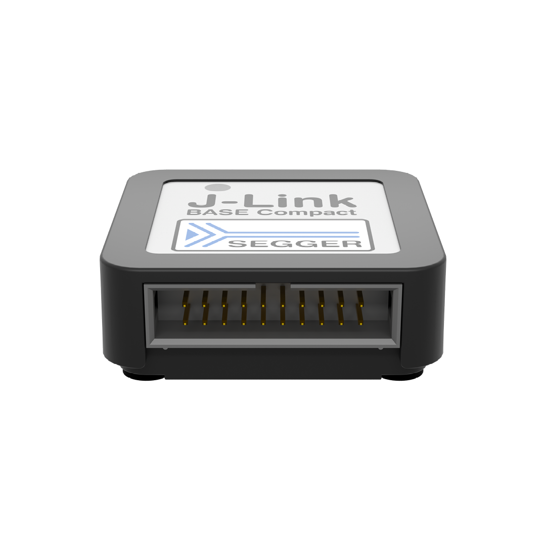
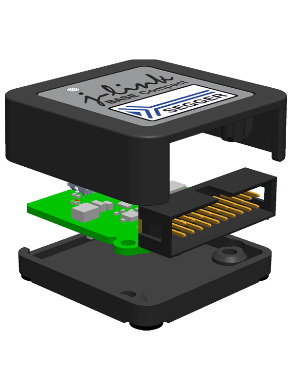
Product images


Technical specifications
| General | |
|---|---|
| Supported OS | Microsoft Windows (x86/x64), Linux (x86/x64/Arm), macOS (x86/Apple Silicon) |
| Electromagnetic compatibility (EMC) | EN 55022, EN 55024 |
| Operating temperature | +5°C ... +60°C |
| Storage temperature | -20°C ... +65 °C |
| Relative humidity (non-condensing) | Max. 90% rH |
| Mechanical | |
| Size of J-Link BASE Classic (without cables) | 100mm x 53mm x 27mm |
| Weight of J-Link BASE Classic (without cables) | 70g |
| Size of J-Link BASE Compact (without cables) | 46mm x 46mm x 17mm |
| Weight of J-Link BASE Compact (without cables) | 20g |
| Available Interfaces | |
| USB interface (J-Link BASE Classic) | USB 2.0 (Hi-Speed); USB Type B |
| USB interface (J-Link BASE Compact) | USB 2.0 (Hi-Speed); USB-C |
| Target interface | JTAG/SWD 20-pin |
| JTAG/SWD Interface, Electrical | |
| Power supply | USB powered Max. 50mA + Target Supply current. |
| Target interface voltage (VIF) | 1.2V ... 5V |
| Current drawn from target voltage sense pin (VTRef) | < 25µA |
| Target supply voltage | 5V (derived from USB voltage) |
| Target supply current | Max. 300mA |
| Reset type | Open drain with 100 Ohms series resistor. Can be pulled low or tristated |
| Reset low level output voltage | VOL <= 10% of VIF |
| For the whole target voltage range (1.2V <= VIF <= 5V) | |
| LOW level input voltage (VIL) | VIL <= 40% of VIF |
| HIGH level input voltage (VIH) | VIH >= 60% of VIF |
| For 1.2V >= VIF <= 3.6V | |
| LOW level output voltage (VOL) with a load of 10 kOhm | VOL <= 10% of VIF |
| HIGH level output voltage (VOH) with a load of 10 kOhm | VOH >= 90% of VIF |
| For 3.6 <= VIF <= 5V | |
| LOW level output voltage (VOL) with a load of 10 kOhm | VOL <= 20% of VIF |
| HIGH level output voltage (VOH) with a load of 10 kOhm | VOH >= 80% of VIF |
| JTAG/SWD Interface, Timing | |
| Target interface speed | Max. 15 MHz |
| SWO sampling frequency | Max. 30 MHz |
| Data input rise time (Trdi) | Trdi <= 20ns |
| Data input fall time (Tfdi) | Tfdi <= 20ns |
| Data output rise time (Trdo) | Trdo <= 10ns |
| Data output fall time (Tfdo) | Tfdo <= 10ns |
| Clock rise time (Trc) | Trc <= 3ns |
| Clock fall time (Tfc) | Trc <= 3ns |
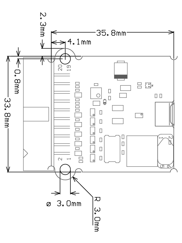
Assembly dimensions
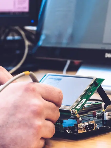
The compact variant of the J-Link BASE is designed to mount securely and unobtrusively into development or end-user equipment. The housing's small size and two mounting holes enable the device to be placed into existing equipment housing or to conserve space for direct mounting to a printed circuit board.
Typical applications for J-Link BASE include test fixtures that are used to automate firmware verification during development, as well as long-term testing setups. It can also be used for integrated firmware reflashing or for service purposes in end equipment, minimizing the number of tools required by service technicians.
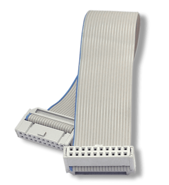
Package content
J-Link BASE Classic

J-Link BASE Compact


FAQ
Can I use J-Flash with J-Link BASE?
No. You either need to purchase the additional license J-Link Upgrade BASE to PLUS if you already own the product, or choose a higher-end model such as J-Link PLUS, J-Link Ultra, or J-Link Pro.
The same applies to the J-Link Flash Breakpoints technology or the Ozone debugger, for instance.
In order to receive a free 30-day trial license, please send an email including your J-Link serial number to: sales@segger.com.
What is the advantage of J-Link versus simple probes such as FTDI-based systems?
J-Link offers numerous advantages: Communication is handled by the probe itself, making it faster and more reliable. Flash loaders are provided by SEGGER or can be created using the Device Support Kit. The debug communication interface RTT is available. All popular IDEs support J-Link across all vendors. With an additional license, an unlimited number of breakpoints in flash memory can be set. In contrast to most simple probes, J-Link supports adaptive clocking as well as SWD and SWO.
Can I use more than one J-Link at the same time on the same machine?
Yes. You can connect an unlimited number of J-Links to your PC. No special configuration is required. Each J-Link is registered with its unique serial number, allowing multiple J-Links to be connected at once.
I have multiple Arm cores in my JTAG chain. How can I debug them (simultaneously) with J-Link?
That’s simple: Two or more debuggers can use the same J-Link simultaneously. Multi-core debugging requires multiple debuggers or multiple instances of the same debugger. You simply need to tell your debugger which device in the scan chain to debug. No additional special settings are required.
Does J-Link support the Embedded Trace Buffer (ETB)?
Yes. J-Link supports ETB on Cortex-M3/M4/M7 and Cortex-A/R devices (if implemented by the target).
Does J-Link support the Micro Trace Buffer (MTB)?
Yes.
Does J-Link support the Embedded Trace Macrocell (ETM)?
No. ETM requires an additional connection to the Arm chip and a CPU with built-in ETM. ETM is supported by the J-Trace product family.
Latest news
Related content
Get in touch with us
Have questions or need assistance? Our Embedded Experts are here to help!
Reach out to us for:
- Licensing quotes
- Technical inquiries
- Project support