J-Flash SPI
Programming tool for SPI flash memories
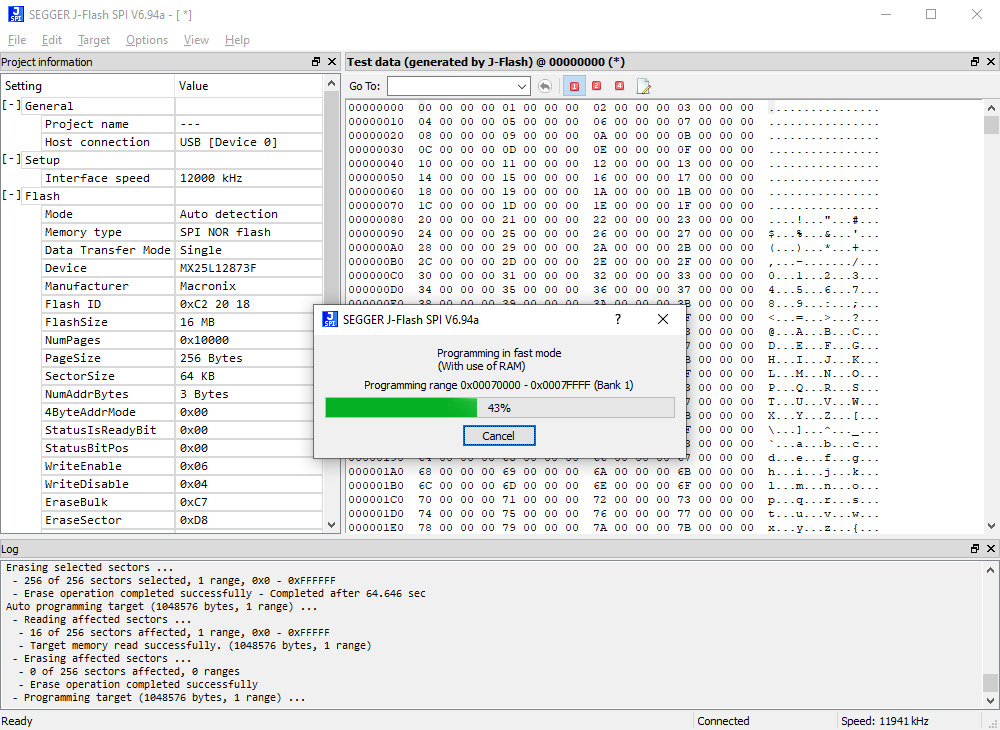
J-Flash SPI is a PC software running on Microsoft Windows systems, Linux or macOS, which allows direct programming of SPI flashes via J-Link or Flasher. The flash is programmed directly via J-Link or Flasher using the SPI protocol, no CPU / MCU in between.
Overview
J-Flash SPI is a PC software running on Microsoft Windows systems, Linux or macOS, which allows direct programming of SPI flashes via J-Link or Flasher. The flash is programmed directly using the SPI protocol, no CPU / MCU in between.
Most common SPI flashes are automatically recognized by their respective ID and can easily be programmed with no further setup / configuration of J-Flash SPI needed to be done by the user.
Key features
- Direct programming of SPI flash via J-Link or Flasher (no CPU / MCU in between)
- Since J-Link and Flasher communicate directly with the flash, even flashes connected to CPUs not supported by J-Link or Flasher can be programmed
- Multi-platform (GUI and command line version available for Windows, Linux and macOS)
- Auto-detection of popular SPI flashes
- Any SPI flash can be supported. All flash parameters can be manually configured/overridden, if required
- Can be controlled via command-line
- Part of the J-Link software and Flasher software.
Software
J-Link BASE requires an upgrade BASE to PLUS, which is available in our web shop.
System requirements
| Supported OS | |
|---|---|
| Windows | Microsoft Windows (x86/x64) |
| macOS | macOS (x86/Apple Silicon) |
| Linux | Linux (x86/x64/Arm) |
20-pin connection
The following table lists the pinout for the SPI interface on J-Link / Flasher (programmer).
| Pin | Signal | Type | Description |
|---|---|---|---|
| 1 | VTref | Input | This is the target reference voltage. It is used to check if the target has power, to create the logic-level reference for the input comparators and to control the output logic levels to the target. It is normally fed from Vdd of the target board and must not have a series resistor. |
| 2 | Not connected | NC | Leave open on target side. |
| 3 | Not connected | NC | Leave open on target side. |
| 5 | DI | Output | Data-input of target SPI. Output of programmer, used to transmit data to the target SPI. |
| 7 | nCS | Output | Chip-select of target SPI (active LOW). |
| 9 | CLK | Output | SPI clock signal. |
| 11 | Not connected | NC | Leave open on target side. |
| 13 | DO | Input | Data-out of target SPI. Input of programmer, used to receive data from the target SPI. |
| 15 | nRESET | Output | Target CPU reset signal (active LOW). Typically connected to the reset pin of the target CPU, which is typically called "nRST", "nRESET" or "RESET". |
| 17 | Not connected | NC | Leave open on target side. |
| 19 | 5V-Supply | Output | This pin can be used to supply power to the target hardware. Older J-Links may not be able to supply power on this pin. |
Pins 4, 6, 8, 10, 12 are GND pins connected to GND in programmer. They should also be connected to GND in the target system.
*On later Flasher and J-Link products like the J-Link Ultra, these pins are reserved for firmware extension purposes. They can be left open or connected to GND.
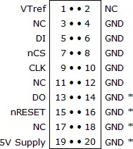
Pinout SPI 20-pin
20-pin QSPI connection
The following table lists the pinout for the quad SPI (QSPI) interface.
| Pin | Signal | Type | Description |
|---|---|---|---|
| 1 | VTref | Input | This is the target reference voltage. It is used to check if the target has power, to create the logic-level reference for the input comparators and to control the output logic levels to the target. It is normally fed from Vdd of the target board and must not have a series resistor. |
| 2 | Not connected | NC | Leave open on target side. |
| 3 | IO1 | I/O | Bi-directional data I/O pin 1 |
| 5 | IO0/DI | I/O | Single: Data-input of target SPI. Output of programmer, used to transmit data to the target SPI. Quad: Bi-directional data I/O pin 0 |
| 7 | nCS | Output | Chip-select of target SPI (active LOW). |
| 9 | CLK | Output | SPI clock signal. |
| 11 | IO2 | I/O | Bi-directional data I/O pin 2 |
| 13 | DO | Input | Single: Data-out of target SPI. Input of programmer, used to receive data from the target SPI. Quad: Must be connected to same signal as pin 3 IO1/DO to guarantee correct operation for temporary single mode transfers during QSPI mode. |
| 15 | nRESET | Output | Target CPU reset signal (active LOW). Typically connected to the reset pin of the target CPU, which is typically called "nRST", "nRESET" or "RESET". |
| 17 | IO3 | I/O | Bi-directional data I/O pin 3 |
| 19 | 5V-Supply | Output | This pin can be used to supply power to the target hardware. Older J-Links may not be able to supply power on this pin. |
Pins 4, 6, 8, 10, 12 are GND pins connected to GND in programmer. They should also be connected to GND in the target system.
*On later Flasher and J-Link products like the J-Link ULTRA, these pins are reserved for firmware extension purposes. They can be left open or connected to GND.
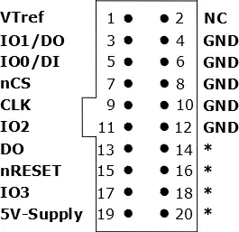
Pinout QSPI 20-pin
J-Link 10-Pin Needle Adapter Connection
The following table lists the pinout for the SPI interface on J-Link / Flasher (programmer) when using the J-Link 10-pin Needle Adapter (model 8.06.04).
| Pin | Signal | Type | Description |
|---|---|---|---|
| 1 | VTref | Input | This is the target reference voltage. It is used to check if the target has power, to create the logic-level reference for the input comparators and to control the output logic levels to the target. It is normally fed from Vdd of the target board and must not have a series resistor. |
| 2 | nCS | Output | Chip-select of target SPI (active LOW). |
| 4 | CLK | Output | SPI clock signal. |
| 5 | 5V-Supply | Output | This pin can be used to supply power to the target hardware. Older J-Links may not be able to supply power on this pin. |
| 6 | DO | Input | Data-out of target SPI. Input of programmer, used to receive data from the target SPI. |
| 7 | Not connected | NC | Leave open on target side. |
| 8 | DI | Output | Data-input of target SPI. Output of programmer, used to transmit data to the target SPI. |
| 9 | Not connected | NC | Leave open on target side. |
| 10 | nRESET | Output | Target CPU reset signal. Typically connected to the RESET pin of the target CPU, which is typically called "nRST", "nRESET" or "RESET". |
Pin 3 is GND pin connected to GND in programmer. It should also be connected to GND in the target system.
Notes regarding nRESET: If there is another device / peripheral that also controls the SPI flash (e.g. a CPU the flash is connected to), nRESET of the programmer should be connected to the reset of the target system or the reset pin of the CPU to make sure that the programmer can keep the CPU in reset while programming the SPI flash.
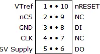
Pinout SPI 10-pin

J-Flash SPI connection
Which SPI flash devices are supported?
J-Flash SPI is able to auto-detect common SPI flashes automatically, via their respective ID. Anyhow, since all flash parameters (size, commands etc.) can also be manually configured by the user, any SPI flash device can be supported. The list of flash devices that are supported by the flash auto-detection of J-Flash SPI can be found here:
List of supported SPI flashes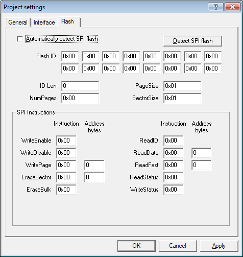
Evaluation hardware
Selecting the right (Q)SPI flash that fits the needs can be a difficult task. There are plenty of different flashes as well as vendors available and creating a hardware for each candidate is time consuming and costly.
To make evaluation of different (Q)SPI flashes a lot easier, we have created a (QSPI) evaluation board.
SPI Flash Evaluator")
Command line version
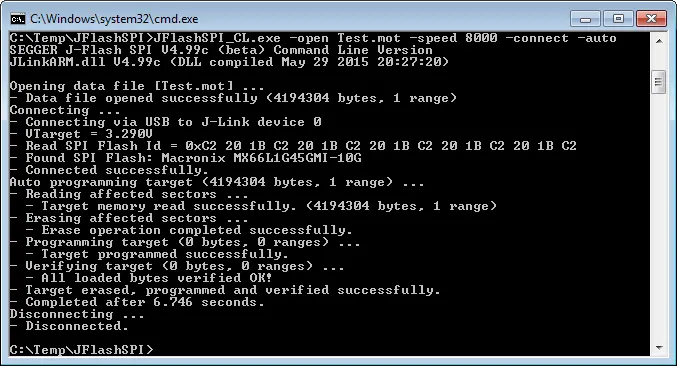
A command line version of J-Flash SPI is available for Windows, Linux and macOS, too. The command line version is also part of the J-Link software and Flasher software. Please note that the GUI version of J-Flash SPI can also be controlled from the command line.
Flash Programming Speed
Due to the high performance and the efficient protocol of J-Link/Flasher, programming speeds up to the max. flash programming specified by the flash vendor, can be achieved.
| Flash device | Programming speed1 |
|---|---|
| ISSI IS25LP128 | 500 KB/s |
| ISSI IS25LD040 | 100 KB/s |
| ISSI IS25LQ080 | 340 KB/s |
| ISSI IS25CD010 | 100 KB/s |
| ISSI IS25CQ032 | 190 KB/s |
| Macronix MX25L3235E | 285 KB/s |
| Macronix MX66L1G45G | 430 KB/s |
| Macronix MX66L51235F | 315 KB/s |
| Micron N25Q128A | 270 KB/s |
| Micron M25P10 | 160 KB/s |
| Micron M25PX16 | 230 KB/s |
| Micron M45PE10 | 230 KB/s |
| Micron M25PE4 | 215 KB/s |
| Spansion S25FL128 | 410 KB/s |
| Spansion S25FL116K | 265 KB/s |
| Winbond W25Q128FV | 340 KB/s |
1 Max. flash programming speed that can be achieved depends on flash device. Flash programming is done in pages and page size as well as page programming time varies from device to device. For more information about the page programming time for a specific flash device, please refer to the appropriate datasheet.