SWD Isolator Box
Optical isolation for SWD interface
- Optical isolation
- Overvoltage protection
- Overcurrent protection
- ESD protection
Overview
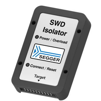
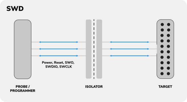
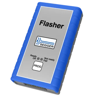
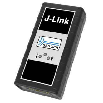
The SWD Isolator Box is inserted into the connection of a J-Link or Flasher and a target board to provide electrical isolation. This is essential when the development or production tools are not connected to the same ground as the application. The SWD Isolator uses high speed digital isolators that allow a very low propagation time between input and output.
Key features
- 1.2 V to 5 V target operation supported
- Powered from probe side
- Overvoltage and overcurrent protection on probe side
- Overvoltage protection on VTref pin of target connector
- 4 LEDs to indicate probe/programmer power, probe/programmer overload, target power, and target RESET
- ESD protection
Use cases
Motor
control
Motor control applications tend to introduce electrical spikes into the system. The isolator protects the debug probe from such hazards.
Production and test
Production and test systems often use a multitude of tools with different characteristics, making it nearly impossible to ensure stable electrical conditions. The isolator shields tools and device under test from each other to minimize impact.
Sensor and analog
Sensor and analog applications require precision where any external signal might disturb correct operation. The isolator shields the measurement system from any potential impact caused by the debug system.
Product images

Technical specification
- Isolation
- 1 kV DC (basic isolation)
- Probe/programmer side interface
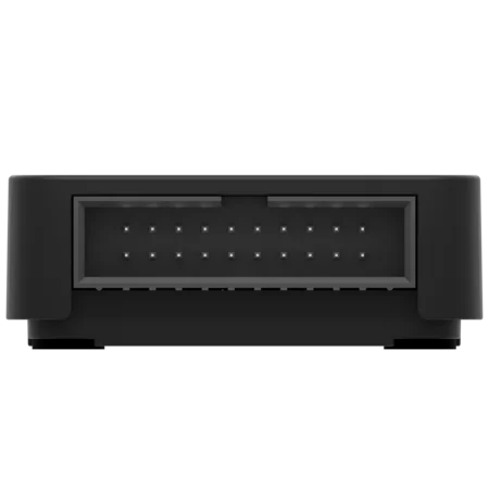
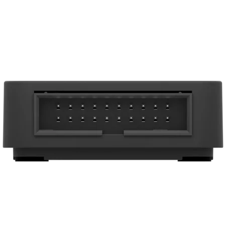
- 20-pin 0.1" male SWD
- Target interface
- 20-pin 0.1" male SWD
- Target signals
- SWCLK, SWDIO, SWO, RESET
- Target interface speed
- Up to 4 MHz
- Target interface voltage
- 1.2 V – 5 V
- Power consumption target side
- <25 µA
- Dimensions
- 73 mm x 46 mm x 19 mm (L x W x H)
- Weight
- 38g
- Operating temperature
- +5 °C ... +60 °C
- Storage temperature
- -20 °C ... + 65°C
- Relative humidity (non-condensing)
- < 90% rH
Connector pinout
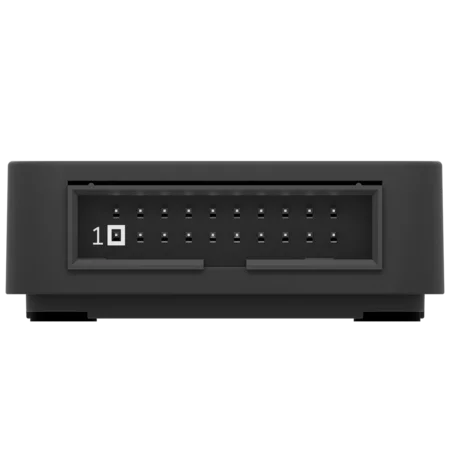
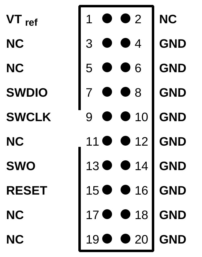
(Connector view)
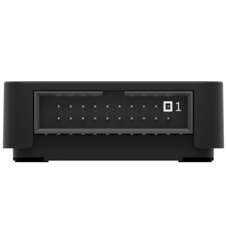
The following table shows the pinout for both connectors of the SWD Isolator:
| Pin | Signal | Type | Description |
|---|---|---|---|
1 | VTref | Input | Reference voltage. The target side of the isolator may draw power over this pin. |
2 | NC | NC | This pin is not connected. |
3 | NC | NC | This pin is not connected. |
5 | NC | NC | This pin is not connected. |
7 | SWDIO | I/O | Bi-directional data pin of SWD. This pin should be pulled high on the target. Typically connected to SWDIO on target CPU. |
9 | SWCLK | Output | SWD clock signal to target CPU. It is recommended that this pin is pulled to a defined state on the target board. Typically connected to SWCLK on target CPU. |
11 | NC | NC | This pin is not connected. |
13 | SWO | Input | SWD data output from target CPU. Typically connected to SWO on target CPU. |
15 | RESET | I/O | Target CPU reset signal. Typically connected to the RESET pin of the target CPU, which is typically called "nRST", "nRESET" or "RESET". |
17 | NC | NC | This pin is not connected. |
19 | VCC / NC | Input / NC | This pin supplies power to the isolator from the debug probe. This pin is not connected on the target side of the isolator. |
Pins 4, 6, 8, 10, 12, 14, 16, 18, 20 are GND pins connected to GND.
Safety
This isolator provides basic isolation only. Do not use with hazardous voltages without further protection measures to avoid risk of electrical shock and fire.
SEGGER isolators provide basic isolation to withstand high voltages as specified in the corresponding technical data section. To ensure personal safety when dealing with potentially hazardous voltages, it is mandatory to provide a second protection measure in place in case the first insulation barrier fails. This is called double or reinforced isolation. How this double isolation can be achieved depends on the use case or application setup. Also check the safety regulations applicable in your country to ensure that all requirements are met.
Package content

FAQ
May I use SWD Isolator with a third party debug probe?
The SWD Isolator has been designed for J-Link and Flasher, but can also be used with other debug probes or programmers with the same pin-out. In this case, you need to make sure that 5 V are supplied to pin 19 of the probe/programmer connector and that yourprobe/programmer is not damaged when applying 5 V to this pin. Do this at your own risk!
May I use the SWD Isolator for JTAG connections as well?
This does not work. The SWD isolator has no connection for the pin used for TDI in JTAG.
May I use the SWD Isolator for compact JTAG (cJTAG) connections?
While the SWD Isolator is specified for the SWD/SWO interface, the SWD Isolator can be used with cJTAG, if the probe uses the same configuration as the J-Link (TMSC on Pin 7, see the target interface description)
Related content
Get in touch with us
Have questions or need assistance? Our Embedded Experts are here to help!
Reach out to us for:
- Licensing quotes
- Technical inquiries
- Project support