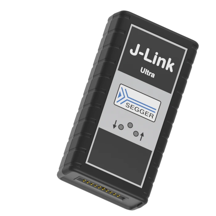
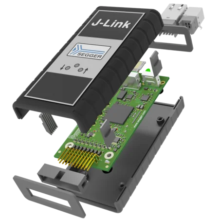
J-Link Ultra
The ultra-fast debug probe in a compact housing
- Ultra-fast JTAG/SWD debug probe
- Uses a fast CPU, a built-in FPGA, and a high-speed USB interface
- Enhanced performance with integrated target power measurement
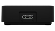
Host Connector
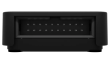
Target Connector
Key features

High download speeds
J-Link Ultra offers download speeds of up to 4 MB/s, ensuring that project development moves forward smoothly and reliably, with minimized download times.
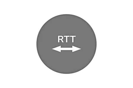
Real Time Transfer
J-Link Ultra offers Real Time Transfer (RTT), which provides a simplified path for information to travel when an application is running. Users can also easily monitor changes in operation. The increased RTT throughput is particularly beneficial for RTT-intensive applications such as SystemView.
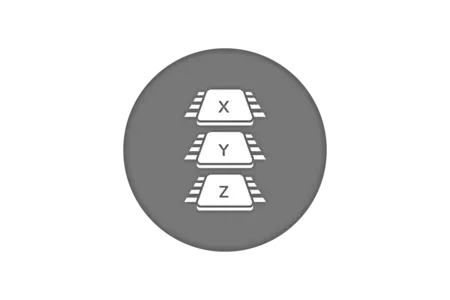
Broad CPU and IDE support
J-Link Ultra works with an extensive range of microcontrollers and integrated development environments (IDEs). It enables users to connect their selected microcontroller with their favorite IDE.
Supported devices
The list of supported manufacturers, families, devices, and SoCs includes tens of thousands of devices in hundreds of device families.
Device not listed? Please don’t hesitate to contact us.
Use cases
Power debugging
J-Link Ultra enables users to perform power debugging, where power consumption is analyzed and matched to the respective code, in order to identify inefficiencies and create design strategies for minimizing power use.
Fast data logging and firmware downloads
J-Link Ultra enhances debugging with download speeds of up to 4 MB/s. This means users can transfer large firmware images rapidly and benefit from an accelerated deployment process. Furthermore, efficient real-time data logging (via RTT), ensures that more data can be logged while the system continues to run. With these capabilities, J-Link Ultra reduces downtime, optimizes debugging workflows, and supports fast iteration cycles, making it an essential tool for developers working with large firmware and complex systems.
J-Link technology
Unlimited Breakpoints
Set as many breakpoints as you need in internal or external flash. Debug thoroughly, even when hardware breakpoints run out.
Monitor Mode
Keep essential system functions running while debugging. Perfect for real-time applications that must stay responsive.
Power Profiling
Measure and optimize energy consumption with high sampling rates and 50 µA resolution. Ideal for battery-powered or energy-harvesting devices.
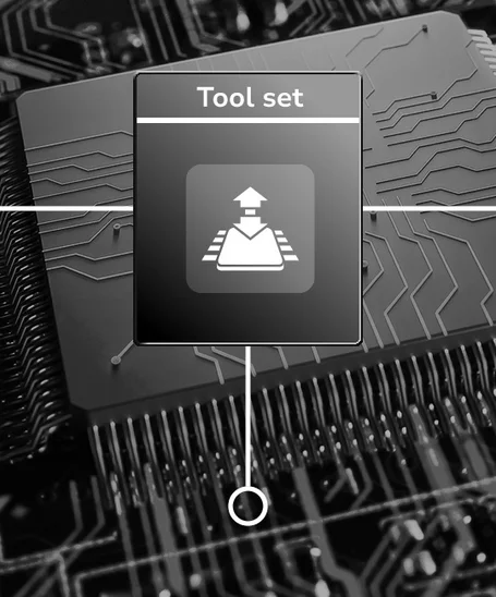
Tool set
J-Link Pro comes with a versatile suite of software tools that enhance its performance and flexibility for debugging and programming. Utilities such as J-Link Commander, J-Link Configurator, and J-Link Remote Server make it a powerful and convenient tool for any development setup. Below are selected highlights from this tool set.

Embedded Studio
J-Link Pro supports SEGGER Embedded Studio as well as virtually all Integrated Development Environments (IDEs), ensuring maximum flexibility in any development setup.
Ozone
It integrates seamlessly with SEGGER’s Ozone debugger, providing a powerful environment for performance analysis, instruction tracing, and code optimization.
J-Flash
J-Flash enables programming of microcontroller internal and external flash memories. Exceedingly versatile, it runs on Microsoft Windows, Linux, and macOS, and it supports Cortex Arm, RX, and RISC-V devices and cores.
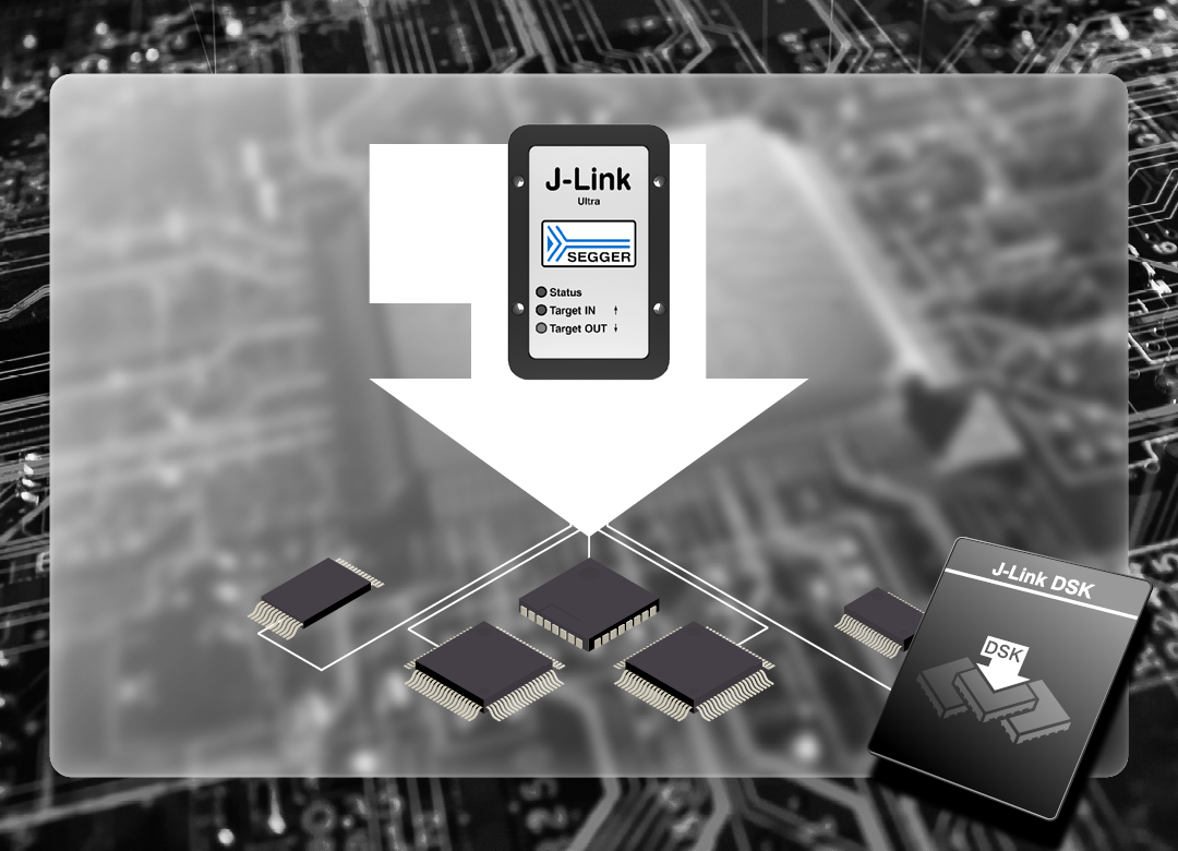
J-Link DSK
The J-Link Device Support Kit (DSK) allows silicon vendors and users to add debug and flash programming support for new devices. A new device typically requires a flash loader and, in some cases, a script defining special connect and reset sequences.
The DSK includes the SEGGER flash loader as well as a collection of example script files for devices that require special handling.

J-Link SDK
The J-Link Software Development Kit (SDK) enables the integration of J-Link and J-Trace support into custom applications. It is used in professional IDEs, such as SEGGER Embedded Studio, to enable direct debugging via J-Link / J-Trace, as well as in customized production utilities. Available for Windows, Linux, and macOS, the SDK can be used with nearly any programming language or solution.
Software
All software is included free of charge, as are licenses for all J-Link-related SEGGER software products, such as J-Link Unlimited Flash Breakpoints, Ozone, RDI, and J-Flash.
The J-Link Software and Documentation Package is available here:
Buyers Guide

J-Link BASE
Ethernet
J-Flash / J-Flash SPI
Unlimited Flash Breakpoints
Ozone
Monitor Mode
RDI
Real Time Transfer (RTT)
Download speed up to 1.0 MByte/sec
Target interface speed up to 15 MHz

J-Link PLUS
Ethernet
J-Flash / J-Flash SPI
Unlimited Flash Breakpoints
Ozone
Monitor Mode
RDI
Real Time Transfer (RTT)
Download speed up to 1.0 MByte/sec
Target interface speed up to 15 MHz

J-Link WiFi
Wireless Connection
J-Flash / J-Flash SPI
Unlimited Flash Breakpoints
Ozone
Monitor Mode
RDI
Real Time Transfer (RTT)
Download speed up to 1.0 MByte/sec
Target interface speed up to 15 MHz

J-Link Ultra
Ethernet
J-Flash / J-Flash SPI
Unlimited Flash Breakpoints
Ozone
Monitor Mode
RDI
Real Time Transfer (RTT)
Download speed up to 4.0 MByte/sec
Target interface speed up to 50 MHz

J-Link Pro
Ethernet
J-Flash / J-Flash SPI
Unlimited Flash Breakpoints
Ozone
Monitor Mode
RDI
Real Time Transfer (RTT)
Download speed up to 4.0 MByte/sec
Target interface speed up to 50 MHz

J-Link Pro PoE
Power over Ethernet
J-Flash / J-Flash SPI
Unlimited Flash Breakpoints
Ozone
Monitor Mode
RDI
Real Time Transfer (RTT)
Download speed up to 4.0 MByte/sec
Target interface speed up to 50 MHz
Customer support
J-Link Ultra comes with one year (12 months) of Basic Support. Beyond that, SEGGER's Extended Coverage gives users the option to extend the hardware warranty and Basic Support for one additional year (12 months) or two additional years (24 months). These options are only available at the time of purchase, either through the Web Shop or upon request; adding coverage at a later date is not possible.
Product images


Technical specifications
| General | |
|---|---|
| Supported OS | Microsoft Windows (x86/x64), Linux (x86/x64/Arm), macOS (x86/Apple Silicon) |
| Electromagnetic compatibility (EMC) | EN 55032, EN 55035 |
| Operating temperature | +5 °C ... +60 °C |
| Storage temperature | -20 °C ... +65 °C |
| Relative humidity (non-condensing) | Max. 90% rH |
| Mechanical | |
| Size (without cables) | 73 mm x 46 mm x 19 mm |
| Weight (without cables) | 40 g |
| Available Interfaces | |
| USB interface | USB 2.0 (hi-speed); USB-C |
| Target interface | JTAG/SWD 20-pin |
| JTAG/SWD Interface, Electrical | |
| Target interface voltage (VIF) | 1.2V ... 5V |
| Current drawn from target voltage sense pin (VTRef) | < 25µA |
| Target supply voltage | 5V (derived from USB voltage) |
| Target supply current | Max. 300 mA |
| Reset type | Open drain with 100 Ohms series resistor. Can be pulled low or tristated |
| Reset low level output voltage | VOL <= 10% of VIF |
| For the whole target voltage range (1.2V <= VIF <= 5V) | |
| LOW level input voltage (VIL) | VIL <= 40% of VIF |
| HIGH level input voltage (VIH) | VIH >= 60% of VIF |
| For 1.2V >= VIF <= 3.6V | |
| LOW level output voltage (VOL) with a load of 10 kOhm | VOL <= 20% of VIF |
| HIGH level output voltage (VOH) with a load of 10 kOhm | VOH >= 80% of VIF |
| For 3.6 <= VIF <= 5V | |
| LOW level output voltage (VOL) with a load of 10 kOhm | VOL <= 20% of VIF |
| HIGH level output voltage (VOH) with a load of 10 kOhm | VOH >= 80% of VIF |
| JTAG/SWD Interface, Timing | |
| Target interface speed | Max. 50 MHz |
| SWO sampling frequency | Max. 100 MHz |
| Data input rise time (Trdi) | Trdi <= 20 ns |
| Data input fall time (Tfdi) | Tfdi <= 20 ns |
| Data output rise time (Trdo) | Trdo <= 10 ns |
| Data output fall time (Tfdo) | Tfdo <= 10 ns |
| Clock rise time (Trc) | Trc <= 3 ns |
| Clock fall time (Tfc) | Trc <= 3 ns |
| Analog power measurement interface | |
| Sampling frequency | 200 kHz |
| Resolution | 50 uA |
Assembly dimensions
Installing debug probes into fixtures has become quite common. To ease preparation, the 3D data of the J-Link housing is available below.
Package content

J-Link Ultra

USB-C cable

20-pin, 0.1" target ribbon cable
Latest news
Related content
Get in touch with us
Have questions or need assistance? Our Embedded Experts are here to help!
Reach out to us for:
- Licensing quotes
- Technical inquiries
- Project support