RX FINE Adapter
Seamless connectivity for J-Link
- Renesas RX target support
- FINE debug interface
Overview

The RX FINE Adapter maps from the standard 20-pin 0.1" connector to the standard 14-pin 0.1" connector defined by Renesas and allows FINE connections to Renesas RX devices.
Pinout & schematics
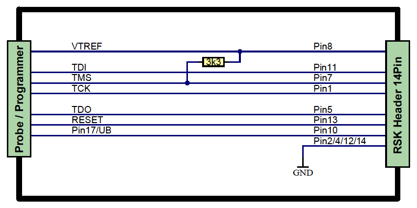
The following functional block diagram illustrates the connections between the debug probe and the target.
Pinout for FINE Connection
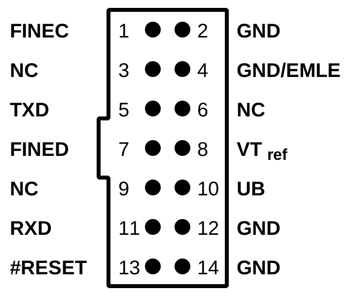
The FINED Signal
The RX FINE Adapter provides a 3k3 pull-up on the FINED line to fulfill the FINE interface specification.
Supported cores via FINE:
- RX111
- RX13T
- RX140
- RX210
- RX21A
- RX220
- RX630
- RX631
- RX63N
- RX64M
- RX65N
- RX651
- RX66T
- RX660
- RX671
- RX72N
CPU Signal RX FINE Adapter Connection
In the following, for the different Renesas RX CPUs the CPU signal <-> RX FINE Adapter signal mapping is described.
RX111 CPUs
- CPU signal / pin name
- RX Adapter pin / signal name
- FINEC / P27
- Pin 1 (FINEC)
- MD_FINED
- Pin 7 (FINED)
- P14
- Pin 10 (UB)
- vRES
- Pin 13 (nRES)
RX130 CPUs
- CPU signal / pin name
- RX Adapter pin / signal name
- MD_FINED
- Pin 7 (FINED)
- VCC CPU (3.3V, 5V, ...)
- Pin 8 (VTref)
- RESn
- Pin 13 (nRES)
- GND
- Pin 2 / 12 / 14 (GND)
- --- (leave open)
- Others
RX210 CPUs
- CPU signal / pin name
- RX Adapter pin / signal name
- SCK1 / P27
- Pin 1 (FINEC)
- MODE / MD_FINED
(via pull-up) - Pin 7 (FINED)
- UB / PC7
- Pin 10 (UB)
- RESET_N / nRES
- Pin 13 (nRES)
RX220 CPUs
- CPU signal / pin name
- RX Adapter pin / signal name
- SCK1 / P27
- Pin 1 (FINEC)
- MODE / MD_FINED
(via pull-up) - Pin 7 (FINED)
- UB / PC7
- Pin 10 (UB)
- RESET_N / nRES
- Pin 13 (nRES)
RX630 CPUs
- CPU signal / pin name
- RX Adapter pin / signal name
- TCK / FINEC / P27
- Pin 1 (FINEC)
- EMLE
- Pin 4 (EMLE)
- MD_FINED
(via pull-up) - Pin 7 (FINED)
- UB / PC7
- Pin 10 (UB)
- RESET_N / RESn
- Pin 13 (nRES)
RX631 / RX63N CPUs
- CPU signal / pin name
- RX Adapter pin / signal name
- TCK / FINEC / P27
- Pin 1 (FINEC)
- EMLE
- Pin 4 (EMLE)
- MD_FINED
(via pull-up) - Pin 7 (FINED)
- UB / PC7
- Pin 10 (UB)
- RESET_N / RESn
- Pin 13 (nRES)
RX63T CPUs
- CPU signal / pin name
- RX Adapter pin / signal name
- TCK / FINEC / P27
- Pin 1 (FINEC)
- EMLE
- Pin 4 (EMLE)
- MD_FINED
(via pull-up) - Pin 7 (FINED)
- RESET_N / RESn
- Pin 13 (nRES)
RX65N / RX651 CPUs
- CPU signal / pin name
- RX Adapter pin / signal name
- TCK / FINEC / P27
- Pin 1 (FINEC)
- MD_FINED
- Pin 7 (FINED)
- UB / PC7
- Pin 10 (UB)
- RESET_N / RESn
- Pin 13 (nRES)
RX66T CPUs
- CPU signal / pin name
- RX Adapter pin / signal name
- MD_FINED
- Pin 7 (FINED)
- UB / P00
- Pin 10 (UB)
- RESET_N / RESn
- Pin 13 (nRES)
RX72N CPUs
- CPU signal / pin name
- RX Adapter pin / signal name
- TCK / FINEC / P27
- Pin 1 (FINEC)
- EMLE
- Pin 4 (EMLE)
- MD_FINED
(via pull-up) - Pin 7 (FINED)
- UB / PC7
- Pin 10 (UB)
- RESET_N / RESn
- Pin 13 (nRES)
Get in touch with us
Have questions or need assistance? Our Embedded Experts are here to help!
Reach out to us for:
- Licensing quotes
- Technical inquiries
- Project support