
Overview
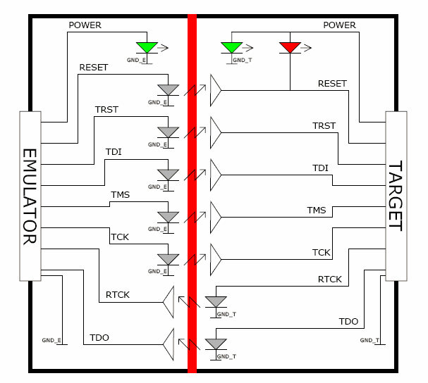
The JTAG Isolator can be connected between J-Link or Flasher and any Arm board that uses the standard 20-pin JTAG Arm connector to provide electrical isolation. This is essential when the development tools are not connected to the same ground as the application. It is also useful to protect the development tools from electrical spikes that often occur in some applications, such as motor control applications. Another typical field of application is the development of products with sensors or other analog circuitry, in which case the target hardware is protected from electrical noise originating from the development PC.

Key features
- Basic isolation (1 kV DC)
- 3.3 V and 5 V target operation supported
- Powered from emulator and target
- JTAG standard 20-pin connection supporting TRST, TDI, TMS, TCK, RTCK, TDO, and RESET signals
- Power consumption on target side: 35 mA typ. / 50 mA max.
- JTAG frequency: Up to 4 MHz
- 3 LEDs to indicate emulator power, target power, and target RESET
Connectors and indicators
The JTAG Isolator uses high speed optocouplers that allow a very low propagation time between input and output. It comes with the following connectors and indicators:
- 20-pin female EMULATOR connector which can be plugged directly into the Flasher
- 20-pin male TARGET connector for connection of the target cable
- Green LED indicating power on the emulator side
- Green LED indicating power on the target side
- Red LED indicating RESET


Target connector
The following table shows the target side pinout of the JTAG Isolator:
| Pin | Signal | Type | Description |
|---|---|---|---|
| 1 | VCC | Input | The target side of the isolator draws power over this pin. |
| 2 | VCC | Input | The target side of the isolator draws power over this pin. |
| 3 | nTRST | Output | JTAG Reset. Output from J-Link / Flasher to the Reset signal on the target JTAG port. Typically connected to nTRST on the target CPU. This pin is normally pulled HIGH on the target to avoid unintentional resets when there is no connection. |
| 5 | TDI | Output | JTAG data input of target CPU. It is recommended that this pin is pulled to a defined state on the target board. Typically connected to TDI on target CPU. |
| 7 | TMS | Output | JTAG mode set input of target CPU. This pin should be pulled up on the target. Typically connected to TMS on target CPU. |
| 9 | TCK | Output | JTAG clock signal to target CPU. It is recommended that this pin is pulled to a defined state on the target board. Typically connected to TCK on target CPU. |
| 11 | RTCK | Input | Return test clock signal from the target. Some targets must synchronize the JTAG inputs to internal clocks. To assist in meeting this requirement, you can use a returned and retimed TCK to dynamically control the TCK rate. J-Link supports adaptive clocking, which waits for TCK changes to be echoed correctly before making further changes. Connect to RTCK if available, otherwise to GND. |
| 13 | TDO | Input | JTAG data output from target CPU. Typically connected to TDO on target CPU. |
| 15 | RESET | I/O | Target CPU reset signal. Typically connected to the RESET pin of the target CPU, which is typically called "nRST", "nRESET" or "RESET". |
| 17 | N/C | N/C | This pin is not connected on the target side of the isolator. |
| 19 | N/C | N/C | This pin is not connected on the target side of the isolator. |
Pins 4, 6, 8, 10, 12, 14, 16, 18, 20 are GND pins connected to GND.
Power supply
Both sides, target and emulator, are totally isolated from each other and separately powered. The target side draws power from pins 1 or 2, the emulator side draws power from pin 19. To avoid current drawn from the target an external power supply can be used to provide power to pins 1 and 2.
How to use the JTAG Isolator with Flashers
In order to use the JTAG Isolator, please follow these steps:
- Plug the Isolator directly into the Flasher.
- Power the Flasher.
- Make sure the green LED on the emulator side is lit. If it is not, please follow the instructions below.
- Connect the target to the target side of the JTAG Isolator.
- If the target is powered, the green LED on the target side should be lit.
The red LED on the target side is lit when a Target RESET is active (low).

How to use the JTAG Isolator with another Arm emulator
The JTAG Isolator has been designed for J-Link, but can also be used with other Arm emulators with the same pin-out. In this case, you should make sure that 5 V are supplied to pin 19 of the emulator connector and that your emulator is not damaged when applying 5 V to this pin. Do this at your own risk!
Safety
This isolator provides basic isolation only. Do not use with hazardous voltages without further protection measures to avoid risk of electrical shock and fire.
SEGGER isolators provide a basic isolation to withstand high voltages as mentioned in the resp. technical data section. To preserve integrity of human beings when dealing with potential hazardous voltages it is mandatory to have a second protection measure in place in case the first insulation barrier fails. This is called double or reinforced isolation. How this double isolation can be achieved depends on the use case or application setup. Also check your local safety related directives valid for your country to make sure all requirements are met.