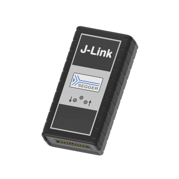
J-Link debug probes
Industry-leading performance and compatibility for embedded development.
- The most widely used family of debug probes worldwide
- Supports a wide range of CPUs and development environments
- Comprehensive feature set for professional embedded development
- 1.Overview
- 2.Key features
- 3.J-Link models
- 3.1.J-Link Pro PoE
- 3.2.J-Link Pro
- 3.3.J-Link Ultra
- 3.4.J-Link PLUS
- 3.5.J-Link WiFi
- 3.6.J-Link BASE
- 3.7.J-Link OB
- 3.8.J-Link EDU Mini
- 4.Supported devices
- 5.Ultra-fast download speed
- 6.Built-in virtual COM port
- 7.Software
- 7.1.Ozone
- 7.2.SystemView
- 7.3.Embedded Studio
- 8.Ecosystem
- 8.1.Wide IDE support
- 8.2.GDB support
- 8.3.LLDB support
- 8.4.OpenOCD support
- 9.Comparison
- 10.Buyers Guide
- 11.Media gallery
- 12.FAQ
Overview
J-Link debug probes are the most popular choice for optimizing the debugging and flash programming experience. Benefit from record-breaking flash loaders, up to 4 MB/s RAM download speed and the ability to set an unlimited number of breakpoints in the flash memory of MCUs.
J-Link also supports a wide range of CPUs and architectures. Everything from single 8051 to mass market Cortex-M to high-end cores like Cortex-A (32- & 64-bit).
J-Link supports directly interfacing SPI flashes, without the need of a CPU between J-Link and the SPI flash (directly communicating via the SPI protocol). J-Link is further supported by all major IDEs, including SEGGER Embedded Studio or Visual Studio Code. See a complete list of supported IDEs here, a complete list of supported devices here and a list of SPI Flashes here.
Key features

High download speeds
J-Link Pro offers download speeds of up to 4 MB/s, ensuring that project development moves forward smoothly and reliably, with minimized download times.
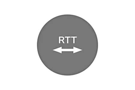
Real Time Transfer
J-Link Pro offers Real Time Transfer (RTT), which provides a simplified path for information to travel when an application is running. Users can also easily monitor changes in operation.
Broad CPU and IDE support
J-Link Pro works with an extensive range of microcontrollers and integrated development environments (IDEs). It enables users to connect their selected microcontroller with their favorite IDE.
J-Link models


Supported devices
The list of supported manufacturers, families, devices, and SoCs includes tens of thousands of devices in hundreds of device families.
Device not listed? Please don’t hesitate to contact us.
Ultra-fast download speed

J-Link makes Flash memory feel almost like RAM. Since it comes with a set of speed-optimized, built-in flash loaders it can easily and quickly be downloaded into flash memory. Take a look below to find out more information.
Built-in virtual COM port
J-Link Pro, J-Link Ultra, J-Link WiFi, J-Link PLUS, J-Link BASE and J-Link OB (if technically possible) come with built-in virtual COM port (VCOM) functionality. This means that in addition to the regular J-Link debug functionality, J-Link will also show up as a COM port in the device manager of the operating system.
Most modern computers don’t have a physical COM port anymore. However, many hardware setups still use UARTs for logging, diagnostics and application control. That’s why a separate COM to USB adapter is needed to get full COM functionality of the target hardware, while debugging at the same time. With J-Link, there’s no need for an additional adapter since J-Link already provides this adaption functionality.
The J-Link VCOM functionality is implemented via SEGGER emUSB-Device, using the CDC-ACM class. J-Link models are shipped with VCOM functionality disabled. It can be enabled via the J-Link Configurator utility. For more information about how to enable VCOM on a J-Link, please refer to the J-Link user guide.
Please note:
- VCOM functionality is not available for the J-Link EDU Mini model.
- VCOM functionality is not available when using the traditional 4-wire JTAG interface for target communication, as Pin 5 is needed as TDI for this interface.
Software
The J-Link Software and Documentation Package available for download includes a significant number of tools that make a developer's job easier and extend the capabilities of J-Link. Almost all J-Link tools have multi-platform support and run on Windows, Linux and macOS.
SystemView
SystemView is a real-time recording and visualization tool for embedded systems, revealing the true runtime behavior of an application. In fact, it even goes far deeper than system insights provided by standard debuggers.
Embedded Studio
Embedded Studio is a complete, all-in-one solution for managing, building, testing, and deploying embedded applications. It is the best solution for embedded C programming: with a Visual Studio-like appearance, embedded engineers get the same intuitive usage PC developers enjoy.
Ecosystem
Wide IDE support
J-Link supports SEGGER’s own software, of course, while also offering support for a host of 3rd-party embedded system development options. To find out more, have a look at the overview of supported IDEs and the 3rd party applications.
GDB support
J-Link can be used in GDB-based setups. The GNU Debugger (GDB) is the de facto standard debugger for development on Linux systems. Over time, it has also become widely adopted in embedded development, even when Linux is not running on the target system. GDB provides a standardized interface/API that can be used by IDEs.
It also defines a standardized protocol, the GDB remote protocol, which enables GDB to communicate with a GDB server that handles the debug probe connected to the target system. The J-Link Software and Documentation Package includes the J-Link GDB Server, enabling the use of J-Link in GDB-based setups.
LLDB support
J-Link can be used with LLDB. Originally, GNU toolchains provided GCC as the compiler and GDB as the debugger. With the introduction of Clang, LLDB emerged as an alternative debugger and successor to GDB. In terms of protocol support, LLDB is backward compatible with GDB, while its IDE API differs slightly.
The J-Link Software and Documentation Package includes the J-Link GDB Server, enabling the use of J-Link in LLDB-based setups.
OpenOCD support
J-Link can be used with OpenOCD (Open On-Chip Debugger). OpenOCD is an open-source software that can interface basically any debug probe. It provides a standardized API, allowing an IDE to support OpenOCD. There are several tutorials on the internet that describe how to use J-Link with OpenOCD.
Please note: OpenOCD is a 3rd party software, so SEGGER cannot provide any guarantees, etc. Using J-Link with OpenOCD bypasses all J-Link specific features like flash programming, unlimited flash breakpoints and the J-Link high debugging speed. OpenOCD will handle J-Link as a simple sequence generator which will affect debug performance. Please also note that using J-Link with OpenOCD is not covered by the standard J-Link support. Support for OpenOCD is provided by the OpenOCD community.
Comparison
The table below shows features of each J-Link debug probe in comparison. If you're interested in trace functionalities in particular, please take a look at SEGGER's J-Trace streaming trace probes.
| J-Link Pro PoE | J-Link Pro | J-Link Ultra | J-Link WiFi | J-Link PLUS | J-Link BASE | |
|---|---|---|---|---|---|---|
| Hardware specifications [1] | ||||||
| Power supply | USB/ Ethernet | USB | USB | USB | USB | USB |
| Download speed into RAM [2] | 4.0 MB/s | 4.0 MB/s | 4.0 MB/s | 1.0 MB/s | 1.0 MB/s | 1.0 MB/s |
| Max. target interface speed | 50 MHz | 50 MHz | 50 MHz | 15 MHz | 15 MHz | 15 MHz |
| Max. SPI interface speed | 50 MHz | 50 MHz | 50 MHz | 12 MHz | 12 MHz | 12 MHz |
| Max. SWO speed | 100 MHz | 100 MHz | 100 MHz | 30 MHz | 30 MHz | 30 MHz |
| Max. VCOM speed/baudrate | 10 MBd | 10 MBd | 10 MBd | 115200 Bd | 115200 Bd | 115200 Bd |
| High Speed Sampling Bandwidth | Unlimited [3] | Unlimited [3] | Unlimited [3] | 1 kHz [4] | 1 kHz [4] | 1 kHz [4] |
| Supported target voltage | 1.2 V - 5 V | 1.2 V - 5 V | 1.2 V - 5 V | 1.2 V - 5 V | 1.2 V - 5 V | 1.2 V - 5 V |
| Host interfaces | ||||||
| Ethernet (including power supply) | ||||||
| Ethernet | ||||||
| USB | ||||||
| WiFi | ||||||
| Target interfaces | ||||||
| cJTAG /JTAG | ||||||
| Target power via USB port | ||||||
| SWD /SWO | ||||||
| Microchip ICSP | ||||||
| Renesas FINE | ||||||
| VCOM | ||||||
| Trace interfaces [5] | ||||||
| ETB/MTB Trace | ||||||
| Cortex ETM Trace | ||||||
| Cortex-A PTM Trace | ||||||
| RISC-V N-Trace BTM | ||||||
| Software features | ||||||
| Flash Download | ||||||
| GDB Server | ||||||
| J-Flash | ||||||
| J-Flash SPI | ||||||
| Ozone | ||||||
| RDI | ||||||
| Real-Time Transfer (RTT) | ||||||
| Unlimited Flash Breakpoints | ||||||
Supported Not supported
[1] The hardware features overview always refers to the current hardware version of the appropriate model. Older hardware versions may not support all of the features mentioned here. For a historical overview for older hardware versions, please refer to the SEGGER Knowledge Base.
[2] The download speeds listed here are the peak download speeds that can be achieved by the particular J-Link model. The actual download speed may be lower as it depends on various factors, such as, but not limited to: The selected debug interface and speed, the CPU core and its operating frequency, other devices in the JTAG chain in case JTAG is used as target interface.
[3] Only limited by the bandwidth of the debug interface. Typical sampling frequency of one variable: > 10 kHz.
[4] Max. sampling frequency is guaranteed for sampling one variable and for appropriate target interface speeds being selected (min. 1 MHz). Sampling more than one variable in parallel, may lead to a smaller max. sampling frequency. When this threshold of sampling frequency decrease is hit, depends on different factors (number of variables to be sampled in parallel, size of each variable, selected target interface speed, etc.).
[5] For full trace support, please refer to SEGGER's J-Trace streaming trace probes.
Buyers Guide

J-Link BASE
Ethernet
J-Flash / J-Flash SPI
Unlimited Flash Breakpoints
Ozone
Monitor Mode
RDI
Real Time Transfer (RTT)
Download speed up to 1.0 MByte/sec
Target interface speed up to 15 MHz

J-Link PLUS
Ethernet
J-Flash / J-Flash SPI
Unlimited Flash Breakpoints
Ozone
Monitor Mode
RDI
Real Time Transfer (RTT)
Download speed up to 1.0 MByte/sec
Target interface speed up to 15 MHz

J-Link WiFi
Wireless Connection
J-Flash / J-Flash SPI
Unlimited Flash Breakpoints
Ozone
Monitor Mode
RDI
Real Time Transfer (RTT)
Download speed up to 1.0 MByte/sec
Target interface speed up to 15 MHz

J-Link Ultra
Ethernet
J-Flash / J-Flash SPI
Unlimited Flash Breakpoints
Ozone
Monitor Mode
RDI
Real Time Transfer (RTT)
Download speed up to 4.0 MByte/sec
Target interface speed up to 50 MHz

J-Link Pro
Ethernet
J-Flash / J-Flash SPI
Unlimited Flash Breakpoints
Ozone
Monitor Mode
RDI
Real Time Transfer (RTT)
Download speed up to 4.0 MByte/sec
Target interface speed up to 50 MHz

J-Link Pro PoE
Power over Ethernet
J-Flash / J-Flash SPI
Unlimited Flash Breakpoints
Ozone
Monitor Mode
RDI
Real Time Transfer (RTT)
Download speed up to 4.0 MByte/sec
Target interface speed up to 50 MHz
Media gallery
FAQ
Can J-Link read back the status of the JTAG pins?
Yes. The status of all pins can be read. This includes the outputs of J-Link as well as the supply voltage, which can be useful for detecting hardware problems on the target system.
What is the maximum download speed into RAM?
The maximum download speed is currently about 4 MB/s for J-Link Pro and J-Link Ultra and about 1 MB/s for J-Link WiFi, J-Link PLUS and J-Link BASE when downloading into RAM. However, the actual speed depends on various factors, such as JTAG, clock speed, host CPU core, etc.
What is the maximum JTAG speed supported by J-Link?
The maximum JTAG speed supported by J-Link Pro and J-Link Ultra is 50 MHz. J-Link PLUS and J-Link BASE support a maximum JTAG speed of 15 MHz.
Which CPUs are supported by J-Link?
J-Link works with devices based on CPU cores from Arm, Cadence, Microchip, Renesas, RISC-V and Silicon Laboratories. For a detailed list, please go to supported CPUs and devices.
The core of my target system could not be recognized automatically. Is there a way to configure my device in order to communicate with J-Link?
Yes. In most cases, J-Link autodetection works reliably and recognizes the core of a device automatically. In some cases, however, J-Link’s autodetection may fail, for example if the core is not present in the JTAG chain by default and needs to be enabled by sending a command to another device in the JTAG chain. In such cases, the J-Link connection sequence can be customized using a J-Link script file that is executed before communication between J-Link and the target system starts. The script file provides maximum flexibility, allowing almost any required target initialization to be supported.
Can I write my own application with J-Link?
Yes. We offer a dedicated Software Development Kit (SDK) that enables access to the full J-Link functionality. Find out more about the available SDKs here.
I have multiple Arm cores in my JTAG chain. How can I debug them simultaneously with J-Link?
This is straightforward. Two or more debuggers can use the same J-Link simultaneously. Multi-core debugging requires multiple debuggers or multiple instances of the same debugger. You simply need to configure your debugger to select the device in the scan chain that you want to debug. No additional special settings are required.
Does J-Link support the Embedded Trace Buffer (ETB)?
Yes. J-Link supports ETB on Cortex-M3, Cortex-M4, Cortex-M7, Cortex M8, and Cortex-A/R devices, provided the feature is implemented by the target device.
Does J-Link support the Micro Trace Buffer (MTB)?
Yes.
Does J-Link support the Embedded Trace Macrocell (ETM)?
No. ETM requires another connection to the ARM chip and a CPU with built-in ETM. ETM is supported by the J-Trace product family.
Latest news
Get in touch with us
Have questions or need assistance? Our Embedded Experts are here to help!
Reach out to us for:
- Licensing quotes
- Technical inquiries
- Project support